GENERAL BLOCK DIAGRAM

approach robotpicture pictures
poweropamppicture motorpicture potpicture
bipolaroutputcircuitpicture powersourcepicture diffampcircuitpicture
dacpicture mcpicture adcpicture
instructionmanual pcpicture sources


APPROACH

The block diagram below represents a general model of the robot ( the process ), a single drive and a control unit. In our case the robot needs four such closed-loop control circuits, one for each degree of freedom

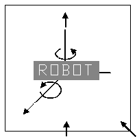
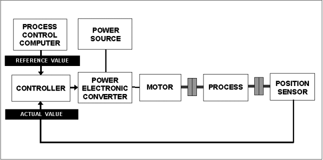
GENERAL BLOCK DIAGRAM FOR MOTOR DRIVE CONTROL

Basically, the microcontroller acts as the control unit: it compares the actual position with the reference value and calculates the output control voltage with a specific digital control algorithm. We considered to different ways of controlling: a digital PID controller and a control using pulsed voltage signals. The latter was to be implemented in case the PID controller would fail to handle the effects of static friction. In the long run we dropped it, because the mechanical structure runned the risk of being damaged by the pulsed drive.

In order to fit the digital controller in the electronic circuit we have to realize some information exchange between the controller and 3 units: the process control computer ( simulated by a set of potentiometers ), the position sensor ( potentiometers ) and the power converter ( a power operational amplifier ), which all operate by means of analog voltages. A digital-to-analog and analog-to-digital converter should manage the exchange.

How to cope with the other units? Our main objective was to preserve what was already present ( the power supply for instance ) and rather using the existing hardware instead of trying to 'reinvent' things. Consequently, analizing and understanding the systems structure and operation was part of the process. We decided to try to incorporate the entire electronic circuitry inside the robots case except the microcontroller, because there was a lack of space and all the more because it would complicate things, instead of making things easier or more user friendly. After having thouroughly tested the electronic circuits and encountering strange phenomena, we conceived printed circuit boards as prototypes, but we took into account that they should fit in properly, if they end up as 'final products'.

Finally, the circuit boards had to be fixed properly inside the robots case. The final test was quite depressing: the manipulator arm was looking somewhat hyperkinetic to say the least. We were not planning to give up THAT soon. Due to a disconnected decoupling capacitor pin, appearently, the whole circuit went unstable. A quick repair and the case was closed... The result of our efforts can be seen and read in "SO?", the conclusive chapter. A more detailed description of all the steps taken can be found in the chapters about the components of the general block diagram. Feel free to wander through...

>>back to general block diagram


THE ROBOT

The robot, a cast-off from the medical sector, has four degrees of freedom to be controlled: a manipulator arm is able to rotate in a horizontal plane and to perform a linear motion along the horizontal and the vertical axis, all three by using a system of guided cables and wheels. Finally, a rotation around the horizontal axis of the manipulator arm itself can be carried out, which adds up to 4 DOF’s, thus 4 DC-motors. The robot had already been examined and tested earlier on, after litterally being picked up from a dusty rack. A great deal of the original hardware, the motor drive electronics included, still remained untouched up to that moment. To start with, the electronic hardware, except the internal power source, the potentiometers and their signal routings had to be removed, because of no use.


view

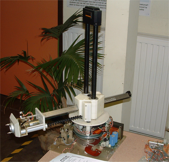
THE ROBOT WITHOUT ITS CASE


mechanism

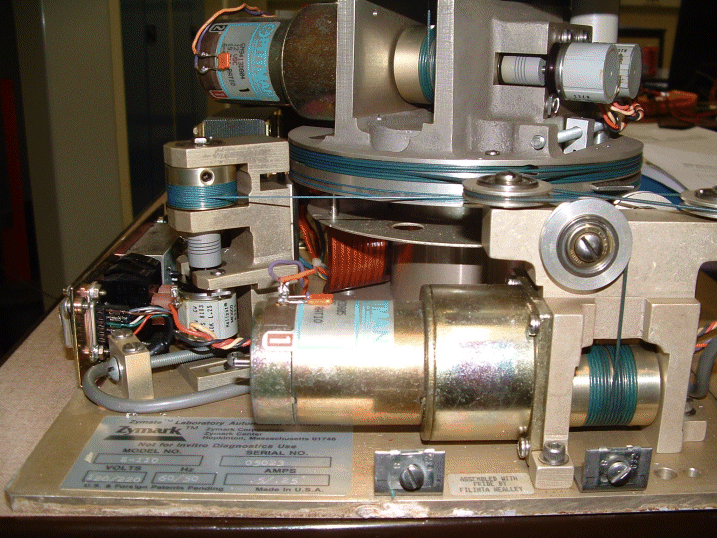
CLOSER LOOK OF THE MECHANISM


zoom

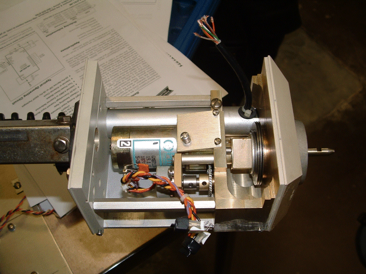
MOTOR AND POTENTIOMETER FOR THE ROTATION AROUND THE HORIZONTAL AXIS


>>back to general block diagram


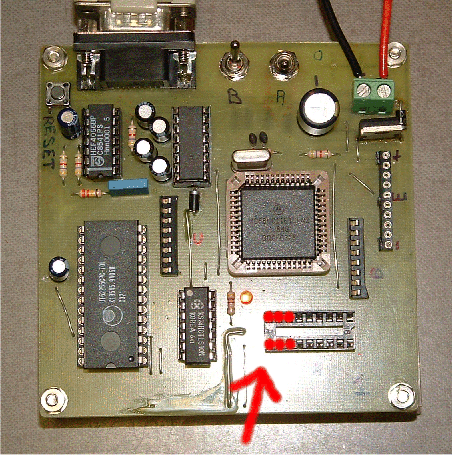
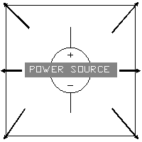
THE POWER SOURCE

The robot contains an internal power supply which generates a rectified +25 and -25 DC-voltage and a +13,8 and -13,8 DC-voltage. The +25 and -25 voltages act as ‘unregulated’ input voltages to a +15V and a -18V voltage regulator to supply the differential amplifier circuit, the bipolar output circuit and the DAC. The +13,8 and -13,8 volt supply the power operational amplifiers, at the same time being connected to +5 and -5 voltage regulators, providing the ADC and the DAC with the required supply voltage. The picture below shows the circuit board with the regulated voltage supply and the socket connecting it to the internal power source of the robot.

regulatedsupply

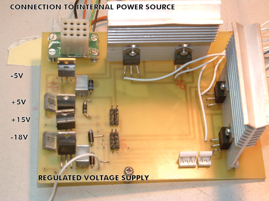
REGULATED VOLTAGE SUPPLY

Some persistence, time and energy was required to sort out the power supply issue. We had to determine whether the existing power supply was able to meet the needs of the DC motors as well as the electronic circuitry. Separating low and high current circuits appeared to be a wise decision.

Besides we've almost scientifically proven the failure of the 7915 voltage regulator series. Having thouroughly tested almost 10 pieces, we found them at the least 'unreliable' and finally came up with a -18V voltage regulator.

ATTENTION: the middle pin of the 78xx and 79xx series voltage regulators is connected to the heat sink! As for the 79xx series, the middle pin is NOT the ground pin ( 78xx series ), BUT the negative voltage input pin. >>back to general block diagram


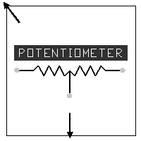
THE POTENTIOMETERS

The position of the manipulator arm is detected by a set of 4 potentiometers, one corresponding with each degree of freedom. The output delivers a variable voltage, depending of the position of the corresponding degree of freedom. Usually, a potentiometer is connected to the mechanical point of interest in a way its output relates to the position of that point in a linear way. In this part we faced an unforeseen and tricky problem: a coupling between the horizontal and vertical degree of freedom, due to the cable system connecting them to their respective motors and potentiometers.

From the beginning, we were aware of this mechanical coupling , but we didn't expect it to have any effect on the potentiometers' behaviour. A movement along the vertical axis, while keeping the position along the horizontal axis steady, results in a variation of the output of the potentiometer corresponding to the horizontal degree of freedom. This means that the potentiometer in question detects a movement which has never taken place, or, to put it in a different way, fails in detecting the horizontal motion that occurs when the vertical degree of freedom moves. The illustration below gives a better view on the problem. Of course this type of false measurement prevents the control algorithm from effectively imposing any 'control' whatsoever. Find more about this problem within chapter 'the differential amplifier circuit'.

As a final configuration, we chose to supply the two pots for rotational motion with 15V and to decouple the two linear motion pots, originally wired in parallel. The pot for vertical motion is connected to -18V and +15V, the pot for horizontal motion to the ground and to +15V. >>back to general block diagram


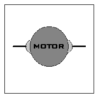
THE DC MOTORS

The different degrees of freedom of the robot are actuated by 4 small DC-motors. In each case the rotation of the motor axis is converted according to the type of motion to be carried out, either with cables and pulley wheels or only cog wheels. Power supply ratings indicate a voltage range from -12V to +12V DC. >>back to general block diagram


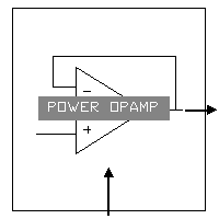
THE POWER OPERATIONAL AMPLIFIERS

We are not able to connect the outputs of the DAC circuits directly to the motors: the current these electronic components can supply is far too small. Therefore, each output of the DAC-circuit is applied to a power OPAMP, configured as a buffer. In this part of the circuit, we get large currents that are not constant! Inductive effects and pollution of the power supply resulted in a failure of the electronic circuit. This problem was solved by putting capacities at the power supply pins of the electronic components and separating the power supply of the power opamps from the low current electronic circuit. ATTENTION: The used power OPAMPs (LM675) put a negative voltage on their heat sink! >>back to general block diagram


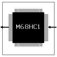
THE MICRO CONTROLLER

The MOTOROLA 68HC11E micro controller was put at our disposal. This device has an 8-bit CPU with a nominal bus speed of 2 MHz, 8 Kbytes of ROM, 512 bytes of EEPROM and 256 bytes of RAM. It also has various on-chip peripheral functions, such as a 16-bit timer system, an 8-bit A/D-converter and an asynchronous as well as a synchronous serial communications interface. For this project, another 32 Kbytes of external RAM were connected to the microcontroller. For more details on this microcontroller, see the Motorola website: http://e-www.motorola.com

We used the internal RAM for the program variables and the external RAM to store the program itself. The timer system was implemented to ensure a constant sampling time. The synchronous serial peripheral interface (SPI) was used to communicate with the other microchips we worked with, namely an 8-channel/12-bit/Analog-to-Digital converter (ADC) and a 4-channel/12-bit/Digital-to-Analog converter (DAC).

The Serial Peripheral Interface (SPI)

SPI is a serial communications protocol supported by many devices. It enables the microcontroller, which acts as a master in our case, to exchange data with its slave devices, namely the ADC and the DAC. Generally, four pins of the microcontroller have to be connected to each slave device. Three of these microcontroller pins are common for all slave devices, namely the MISO-pin (Master In Slave Out), the MOSI-pin (Master In Slave Out) and the SCK-pin (Serial ClocK). The fourth is the SS-pin (Slave Select), which has to be unique for each slave device because it serves to select the device the microcontroller has to communicate with.

Any data-exchange using SPI takes place as follows: first, the SS-pin of the slave is set to low. Before the exchange, the data from each device (master and slave) are stored in a register in the corresponding device (8-bit registers in our case). With each rising (or falling) slope of the clock signal, the data are shifted one bit via the MISO and the MOSI connection. This way, the slave data will be in the master register and the master data will be in the slave register after 8 clock cycles, thus completing the data transfer. >>back to general block diagram


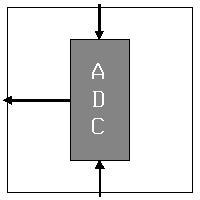
THE ANALOG-to-DIGITAL CONVERTER

The MAX1270 - Multirange, +5V, 8-Channel, Serial 12-Bit ADC serves the purpose. We made use of free on line sample request possibilities at www.maxim-ic.com. In order to meet the specifications a 12-bit converter was preferable to the 8-bit adc present within the microcontroller-chip. The 4 analog voltage signals, representing the mechanical status of the robot (4 DOF's), and the 4 analog reference values, imposed by the user through bnc-cables, are converted into twelve bit digital numbers. The digital actual and reference values are then to be sent to the microcontroller by means of a data transfer protocol called SPI (...read more about it in chapter "the micro controller" and " the assembler code" ).

The MAX1270 has software-controllable input ranges for each channel. >>back to general block diagram


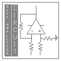
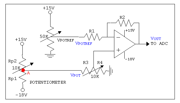
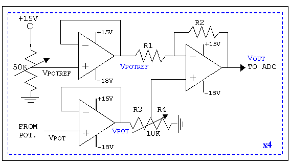
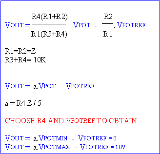
THE DIFFERENTIAL AMPLIFIER CIRCUIT

In order to achieve maximal accuracy, the voltage sweep - or output range - of each potentiometer should nicely fit the chosen input range of each ADC input channel. We’ve chosen 3 quite straightforward ways to do so. The first one is adjusting the potentiometer’s voltage supply to have an output variation of approximately 10 V. The second and third one, shifting and ‘fine tuning’ the voltage range, is being done by differential amplifiers. As you noticed in the chapter about the potentiometers, we tried out an adc input channel range of [-10,+10]V. A malfunction appeared, so we concluded that the 8 input channels of the MAX 1270 should be configured in the same range [0,+10]V.

The initial circuit consisted of 4 differential amplifiers with input signals directly connected. Due to the amplifiers low input impedance, currents vary with changing potentiometer impedance, causing an additional voltage drop and thus distorting the amplifiers input voltage. We beared in mind that this problem could occur, but having tested the rotational degree of freedom and the lineair motion in the horizontal plane the robot seemed to behave nicely , so we carried on. The potentiometer for horizontal motion, however, suffered from the unforeseen coupling, explained before, which did not appear until we altered the vertical position. Its voltage sweep at the amplifiers output varied from [0,+10]V below to [-10,0]V with the manipulator arm in it's highest vertical position.

We assumed the coupling to be lineair and tried to implement a correction in assembler code, to the horizontal position signal, depending on the vertical position signal value. We noticed that the voltage sweep varied with the vertical position as well. We then measured the variation of the horizontal potentiometer signal at the output of the differential amplifier when altering the horizontal position. The fit gave us a parabola. Initially, we inclined to blaming the mechanical part. Maybe the square in the equation emerged from Phytagoras'theorem and the geometry of the system of cables was its logical proof? It began to look like a worst case scenario, leaving us with two ultimate solutions.Trying to find - by calculation or by measurement - the complex relationship between the voltage signal and the actual position and using the inverse function to implement a correction in the software part, or fixing another 'brand new' potentiometer on the manipulator. Ir. Ronald Van Ham, teaching assistant, took care of the latter, as you can see below.


newwheel

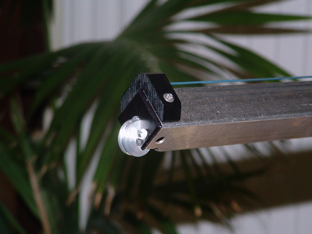
WHEEL FOR THE NEW POTENTIOMETER


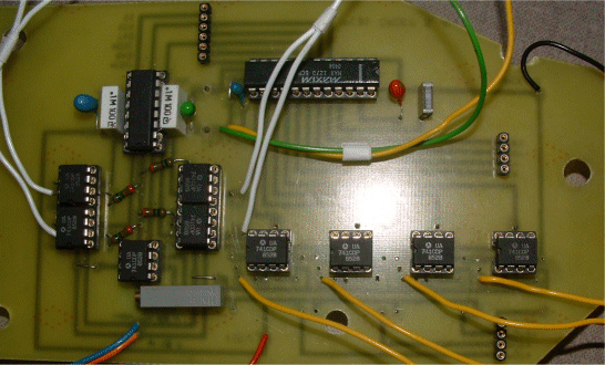
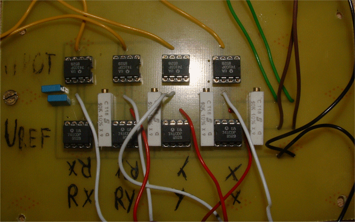
Measurements of the potentiometers impedance variation and an examination of the system of cables and wheels however, reveiled that the electronic circuit HAD to be the main cause. The figures below explain the input impedance problem in further detail. The most straightforward solution was to add a buffer amplifier for each signal, Vpot and Vpotref. Therefore we designed a new circuit board.


badcircuit

FIRST PROTOTYPE OF DIFFERENTIAL AMPLIFIER CIRCUIT


calculation

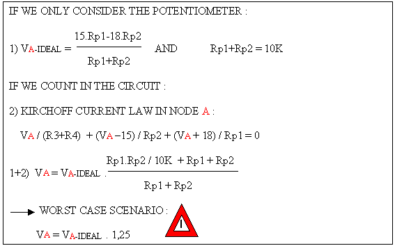
CALCULATION OF THE INFLUENCE OF THE AMPLIFIERS INPUT IMPEDANCE


improvedcircuit

IMPROVED DIFFERENTIAL AMPLIFIER CIRCUIT


tuning

HOW TO TUNE THE CIRCUIT?


THE ORIGINAL DESIGN


THE ADDITIONAL BUFFER CIRCUIT


Finally, we connected the horizontal motion pot to the ground and to +15V.The horizontal sweep is now reduced to [0,+5]V below and [+5,+10]V at the top. The numerical voltage signal correction, taking place in the microcontroller, solves the mechanical coupling problem. In spite of the slight loss of resolution and a few imperfections, we managed to solve the problem at last. If altered due to vertical motion, we clearly notice the horizontal reference position being restored. The controller controls after all... >>back to general block diagram


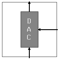
THE DIGITAL-to-ANALOG CONVERTER

This converter is a MAX536 - Calibrated, Quad, 12-Bit Voltage-Output DAC. Again, we made use of free on line sample request possibilities on www.maxim-ic.com.It's purpose is to convert the digital controller output signal to an analog voltage driving the DC motors. The latter should cover the desired range of -10V to +10V for proper driving capabilities. In a typical operating circuit the ADC output channels however, vary from 0V to the full-scale output voltage, set by a user defined reference voltage (maximum Vcc-4V). We chose 10V as a reference and configured the outputs for bipolar operation by using operational amplifiers in a voltage-shifter circuit. >>back to general block diagram


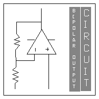
THE BIPOLAR OUTPUT CIRCUIT

As mentioned in the chapter about the DAC, this circuit shifts the voltage output range. The following diagram explains it's operation and structure. The circuits outputs are connected to the input pins of the power opamps.


voltageshifting

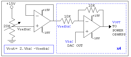
VOLTAGE SHIFTING CIRCUIT DIAGRAM AND OPERATION


>>back to general block diagram


THE ASSEMBLER CODE

THE PROGRAM

The microcontroller programming language is Motorola 68HC11 assembler. This is a low-level-language which is a little more difficult to use and to read than high-level-languages, and which is specific for this type of microcontroller. In the following, the main program and the subroutines are briefly discussed. More detailed explanation on the subroutines can be found in the comments in the program code.

- Main program

In the main program, the variables are initialised and various subroutines are called upon to configure the timer and the SPI, to get data from the ADC, to process this data and to send the processed data to the DAC. There is also some code that corrects the value of the measured position of the horizontal Degree Of Freedom (DOF), using the value of the measured position of the vertical DOF. This is necessary because the value of the measured position of the horizontal DOF varies when the vertical DOF moves, due to a coupling between these two DOF's, as explained in the chapters about the hardware.

- InitSPI subroutine

This subroutine enables and configures the Serial Peripheral Interface for communications with the slave devices.

- InitRTI subroutine

This subroutine configures the Real Time Interrupt (RTI). RTI is a function of the timer system that periodically generates an interrupt. Here it is configured to generate the interrupt every 4.10 milliseconds. Each time this interrupt occurs, a counter is increased. This counter is then compared with a certain value in the main program. When it reaches this value, data is sent to the D/A-converter, thus obtaining a constant sampling time.

- GetFromADC subroutine

This subroutine implements the SPI to get data from the A/D-converter. The input variable adccb is used to select the ADC-channel. The received data is stored in the variables adlsb (Least Significant Bits or LSB's) and admsb (Most Significant Bits or MSB's).

- SendToDAC subroutine

This subroutine implements the SPI to send data to the D/A-converter. The input variables damsb and dalsb contain the data to be sent (dalsb and damsb 4 LSB's) as well as the output channel selection (damsb 4 MSB's).

- Multiplication subroutine

This subroutine multiplies two 16-bit unsigned numbers. The output of this subroutine is a 32-bit number. This subroutine was written because there was only an instruction available to multiply two 8-bit numbers, while we needed to be able to easily multiply at least 12-bit numbers.

- Addition subroutine

This subroutine adds two numbers, whose absolute values are stored in two input variables and whose signs are stored in a separate input variable. This subroutine does not check for overflows, because normally it can't occur in this program that the result exceeds the 32-bit capacity. This subroutine was written to be able to easily add and subtract the results of the Multiplication subroutine.

- PIDController subroutine

This is the most important subroutine, as it processes the input data, namely the reference and actual value of the position of a DOF of the robot, to obtain a value for the signal which is applied to the DC-motors on the robot. This subroutine is, as its name says, a digital implementation of a classical analogue PID-controller (Proportionate-Integral-Differential).
>>back to general block diagram


THE CODE

The complete assembler code, comments included.

If you prefer to download an easy to read and more structured .txt file CLICK HERE .

*****************************************
* Kris Van den Abeele - 22/04/2004 *
*****************************************
*************************************************
* Register Names *
*************************************************
REGBLK EQU $1000 * Starting address for 68HC11 register block
PORTD EQU $08 * PORT D memory location
DDRD EQU $09 * PORT D Data Direction Register memory location
SPCR EQU $28 * Serial Peripheral Condition Register memory location
SPSR EQU $29 * Serial Peripheral Status Register memory location
SPDR EQU $2A * Serial Peripheral Data Register memory location
TMSK2 EQU $24 * Timer interrupt MaSK register 2 memory location
TFLG2 EQU $25 * Timer interrupt FLaG register 2 memory location
PACTL EQU $26 * Pulse Accumulator ConTroL register memory location

*************************************************
* Constant declarations *
*************************************************
cmpcoun EQU $06 * to compare with counter
daczero EQU $0800 * value corresponding with DAC-circuit zero voltage output
corfact EQU $0110 * used to correct actval3, radix point to the left of bit 7
A1 EQU $3800 * $3800 controller 1 A factor, radix point to the left of bit 7
B1 EQU $1C00 * $1C00 controller 1 B factor, radix point to the left of bit 7
C1 EQU $0000 * $0000 controller 1 C factor, radix point to the left of bit 7
A2 EQU $3000 * $3000 controller 2 A factor, radix point to the left of bit 7
B2 EQU $1800 * $1800 controller 2 B factor, radix point to the left of bit 7
C2 EQU $0008 * $0008 controller 2 C factor, radix point to the left of bit 7
A3 EQU $0C00 * controller 3 A factor, radix point to the left of bit 7
B3 EQU $0300 * controller 3 B factor, radix point to the left of bit 7
C3 EQU $0001 * controller 3 C factor, radix point to the left of bit 7
A4 EQU $1E00 * controller 4 A factor, radix point to the left of bit 7
B4 EQU $0C00 * controller 4 B factor, radix point to the left of bit 7
C4 EQU $001E * controller 4 C factor, radix point to the left of bit 7
*********************************************************************************
* Het volgende kan nog gewijzigd geworden in functie van de eevoudigste layout *
* voor de schakeling van de MAX1270. *
*********************************************************************************
*********************************************************************************
* For explanation on the control byte, see subroutine GetFromAC comments *
*********************************************************************************
cbact4 EQU %10001000 * control byte for adc, channel 0: PID3 act val linear x
cbact1 EQU %10011000 * control byte for adc, channel 1: PID2 act val linear y
cbact2 EQU %10101000 * control byte for adc, channel 2: PID1 act val rotation y
cbact3 EQU %10111000 * control byte for adc, channel 3: PID4 act val rotation x
cbref3 EQU %11001000 * control byte for adc, channel 4: PID3 ref val linear x
cbref2 EQU %11011000 * control byte for adc, channel 5: PID2 ref val linear y
cbref1 EQU %11101000 * control byte for adc, channel 6: PID1 ref val rotation y
cbref4 EQU %11111000 * control byte for adc, channel 7: PID4 ref val rotation x
daccb3 EQU %00110000 * control bits for dac, channel A: PID3 out val linear x
daccb2 EQU %01110000 * control bits for dac, channel B: PID2 out val linear y
daccb1 EQU %10110000 * control bits for dac, channel C: PID1 out val rotation y
daccb4 EQU %11110000 * control bits for dac, channel D: PID4 out val rotation x

ORG $0000 * internal RAM used for data

*************************************************
* Variable declarations *
*************************************************
*********************************
* Main program variables *
*********************************
counter RMB 1 * used for timing (sample time)
int1lsb RMB 1 * 8 lsb's of 24-bit integral for 1st controller, initialise $08
int1lsa RMB 1 * 8 middle bits of 24-bit integral for 1st controller, initialise $00
int1msb RMB 1 * 8 msb's bits of 24-bit integral for 1st controller, initialise $00
int2lsb RMB 1 * 8 lsb's of 24-bit integral for 2nd controller, initialise $08
int2lsa RMB 1 * 8 middle bits of 24-bit integral for 2nd controller, initialise $00
int2msb RMB 1 * 8 msb's bits of 24-bit integral for 2nd controller, initialise $00
int3lsb RMB 1 * 8 lsb's of 24-bit integral for 3rd controller, initialise $08
int3lsa RMB 1 * 8 middle bits of 24-bit integral for 3rd controller, initialise $00
int3msb RMB 1 * 8 msb's bits of 24-bit integral for 3rd controller, initialise $00
int4lsb RMB 1 * 8 lsb's of 24-bit integral for 4th controller, initialise $08
int4lsa RMB 1 * 8 middle bits of 24-bit integral for 4th controller, initialise $00
int4msb RMB 1 * 8 msb's bits of 24-bit integral for 4th controller, initialise $00
error11 RMB 2 * PIDController 1 error at the previous sampling period
error12 RMB 2 * PIDController 2 error at the previous sampling period
error13 RMB 2 * PIDController 3 error at the previous sampling period
error14 RMB 2 * PIDController 4 error at the previous sampling period
bools1 RMB 1 * PIDController 1 bools variable
bools2 RMB 1 * PIDController 2 bools variable
bools3 RMB 1 * PIDController 3 bools variable
bools4 RMB 1 * PIDController 4 bools variable
*****************************************
* SendToDAC subroutine variables *
*****************************************
damsb RMB 1 * D/A converter MSB (input)
dalsb RMB 1 * D/A converter LSB (input)
*****************************************
* GetFromADC subroutine variables *
*****************************************
adccb RMB 1 * A/D converter Control Byte (input)
admsb RMB 1 * A/D converter MSB (output)
adlsb RMB 1 * A/D converter LSB (output)
*****************************************
* PIDController subroutine variables *
*****************************************
refval RMB 2 * reference value (input)
actval RMB 2 * actual value (input)
factorA RMB 2 * 16-bit factor, radix point to the left of bit 7 (input)
factorB RMB 2 * 16-bit factor, radix point to the left of bit 7 (input)
factorC RMB 2 * 16-bit factor, radix point to the left of bit 7 (input)
bools RMB 1 * used to store the sign of numbers (input) (output)
intlsbb RMB 1 * 8 lsb's of 24-bit integral (input) (output)
intlsba RMB 1 * 8 middle bits of 24-bit integral, initialise with $00 (input) (output)
intmsbb RMB 1 * 8 msb's bits of 24-bit integral, initialise with $00 (input) (output)
error0 RMB 2 * error at sample interval n-0
error1 RMB 2 * error at sample interval n-1, intialise with value = 0 (input) (output)
pint RMB 2 * rounded integral term
pidout RMB 2 * PID-controller output value (output)
errsum RMB 2 * sum of errors current and previous sample interval
pdlsb RMB 2 * 8 LSB's of sum of proportional and differential part of PID-output
pdmsb RMB 2 * 8 MSB's of sum of proportional and differential part of PID-output
tmpbmsb RMB 2 * intermediate term
tmpblsb RMB 2 * intermediate term
*****************************************
* Multiplication subroutine variables *
*****************************************
factor1 RMB 2 * first factor for multiplication (input)
factor2 RMB 2 * seconde factor for multiplication (input)
term1l RMB 1 * intermediate term
term4m RMB 1 * intermediate term
tmpterm RMB 2 * intermediate term
resulta RMB 1 * 8 msb's of result (output)
resultb RMB 1 * 8 middle msb's of result (output)
resultc RMB 1 * 8 middle lsb's of result (output)
resultd RMB 1 * 8 lsb's of result (output)
*********************************
* Addition subroutine variables *
*********************************
trm1lsb RMB 2 * 16 LSB's of 1st input term (input)
trm1msb RMB 2 * 16 MSB's of 1st input term (input)
trm2lsb RMB 2 * 16 LSB's of 2nd input term (input)
trm2msb RMB 2 * 16 MSB's of 2nd input term (input)
sumlsb RMB 2 * 16 LSB's of sum (output)
summsb RMB 2 * 16 MSB's of sum (output)
* bools RMB 1 * used to store the sign of numbers (input) (output)
tmpadd1 RMB 1 * intermediate term
tmpadd2 RMB 1 * intermediate term
*************************************************************************************************
*************************************************
* Main Program *
*************************************************

ORG $8000 * External RAM used for program
Main
LDS #$00FF * Load stack pointer at $FF, going down
LDX #REGBLK

*****************************************
* Configure Serial Peripheral Interface *
*****************************************
JSR InitSPI
*****************************************
* initialise Real Time Interrupt *
*****************************************
JSR InitRTI
*****************************************
* initialise controller integrals at 0 *
*****************************************
LDD #daczero
STAA int1msb
STAA int2msb
STAA int3msb
STAA int4msb
STAB int1lsa
STAB int2lsa
STAB int3lsa
STAB int4lsa
CLR int1lsb
CLR int2lsb
CLR int3lsb
CLR int4lsb
*****************************************
* initialise previous errors at 0 *
*****************************************
LDD #$0000
STD error11
STD error12
STD error13
STD error14

* PID-controller 1
loop LDAA #cbref1
STAA adccb * control byte for ref value used by GetFromADC
JSR GetFromADC * get reference value for PID1 from ADC
LDAA admsb * 4 MSB's from reference value stored in admsb
LDAB adlsb * 8 LSB's from reference value stored in adlsb
STD refval * store 12-bit reference value in refval
LDAA #cbact1
STAA adccb * control byte for act value used by GetFromADC
JSR GetFromADC * get actual value for PID1 from ADC
LDAA admsb * 4 MSB's from actual value stored in admsb
LDAB adlsb * 8 LSB's from actual value stored in adlsb
STD actval * store 12-bit actual value in refval
LDD #A1
STD factorA
LDD #B1
STD factorB
LDD #C1
STD factorC
LDAA int1lsb
STAA intlsbb
LDAA int1lsa
STAA intlsba
LDAA int1msb
STAA intmsbb
LDD error11
STD error1
LDAA bools1
STAA bools
JSR PIDController * calculate PID-controller 1 output
LDAA intlsbb
STAA int1lsb
LDAA intlsba
STAA int1lsa
LDAA intmsbb
STAA int1msb
LDD error1
STD error11
LDAA bools
STAA bools1
WAITA LDAA counter * wait to ensure constant sample time
CMPA #cmpcoun * 6 periods of 4.10 ms have past --> send data to DAC
BLO WAITA
CLR counter
LDD pidout
ORAA #daccb1 * damsb 4 MSB's: DAC control bits
STAA damsb * store 8 MSB's from PID1 output in damsb
STAB dalsb * store 8 LSB's from PID1 output in dalsb
JSR SendToDAC
* PID-controller 2
LDAA #cbref2
STAA adccb * control byte for ref value used by GetFromADC
JSR GetFromADC * get reference value for PID2 from ADC
LDAA admsb * 4 MSB's from reference value stored in admsb
LDAB adlsb * 8 LSB's from reference value stored in adlsb
STD refval * store 12-bit reference value in refval
LDAA #cbact2
STAA adccb * control byte for act value used by GetFromADC
JSR GetFromADC * get actual value for PID2 from ADC
LDAA admsb * 4 MSB's from actual value stored in admsb
LDAB adlsb * 8 LSB's from actual value stored in adlsb
STD actval * store 12-bit actual value in refval
LDD #A2
STD factorA
LDD #B2
STD factorB
LDD #C2
STD factorC
LDAA int2lsb
STAA intlsbb
LDAA int2lsa
STAA intlsba
LDAA int2msb
STAA intmsbb
LDD error12
STD error1
LDAA bools2
STAA bools
JSR PIDController * calculate PID-controller 2 output
LDAA intlsbb
STAA int2lsb
LDAA intlsba
STAA int2lsa
LDAA intmsbb
STAA int2msb
LDD error1
STD error12
LDAA bools
STAA bools2
WAITB LDAA counter * wait to ensure constant sample time
CMPA #cmpcoun * 6 periods of 4.10 ms have past --> send data to DAC
BLO WAITB
CLR counter
LDD pidout
ORAA #daccb2 * damsb 4 MSB's: DAC control bits
STAA damsb * store 8 MSB's from PID2 output in damsb
STAB dalsb * store 8 LSB's from PID2 output in dalsb
JSR SendToDAC
* PID-controller 3
LDAA #cbref3
STAA adccb * control byte for ref value used by GetFromADC
JSR GetFromADC * get reference value for PID3 from ADC
LDAA admsb * 4 MSB's from actual value stored in admsb
LDAB adlsb * 8 LSB's from actual value stored in adlsb
STD refval * store 12-bit reference value in refval
*********************************************************************************
* The actual value measurement of this degree of freedom has to be corrected, *
* using the actual value of the second degree of freedom. *
*********************************************************************************
*********************************
* Begin correction of actval *
*********************************
LDAA #cbact2
STAA adccb
JSR GetFromADC
LDAA admsb
LDAB adlsb
COMA * the lower position of the 2nd degree of freedom
ANDA #$0F * corresponds to the maximum actval2 value
COMB * 4 msb's of actval must be zero
STD factor1
LDD #corfact
STD factor2
JSR Multiplication
* shift right 8 bits to perform a division by 2^8, round the resulting value
LDAA resultd * Multiplication subroutine output 8 LSB's
CMPA #$80
BLO TrcCor
LDAA resultb
LDAB resultc
ADDD #$0001
STD trm1lsb
LDAA #$00
LDAB resulta
ADCB #$00
JMP EndTrCr
TrcCor LDAA resultb
LDAB resultc
STD trm1lsb
LDAA #$00
LDAB resulta
EndTrCr STD trm1msb
* Get measured actual value of the third degree of freedom
LDAA #cbact3
STAA adccb * control byte for act value used by GetFromADC
JSR GetFromADC * get actual value for PID3 from ADC
LDAA admsb * 4 MSB's from actual value stored in admsb
LDAB adlsb * 8 LSB's from actual value stored in adlsb
CLC * 2nd DOF at low pos ==> 5V < 3rd DOF pos measurement > 10V
ROLB * ==> $0800 < digital position value < $0FFF ==> multiply by
ROLA * 2 to get a variation of $0FFF
STD trm2lsb
LDD #$0000
STD trm2msb
LDAA #%11000000 * both terms are positive
STAA bools
JSR Addition
LDD summsb
CPD #$0000 * 16 most significant bits should be zero...
BNE Proble1
LDD sumlsb
CPD #$1000 * corfact has the correct value ==> sumlsb >= $1000
BLO Proble2
CLC * 0V actual value for 3rd degree of freedom corresponds
SUBD #$1000 * with $0000 ADC-output --> corfact has $1000 value
JMP EndCorr
Proble1 LDD #$0FFF
JMP EndCorr
Proble2 LDD #$0000
EndCorr STD actval
*********************************
* End correction of actval. *
*********************************
LDD #A3
STD factorA
LDD #B3
STD factorB
LDD #C3
STD factorC
LDAA int3lsb
STAA intlsbb
LDAA int3lsa
STAA intlsba
LDAA int3msb
STAA intmsbb
LDD error13
STD error1
LDAA bools3
STAA bools
JSR PIDController * calculate PID-Controller 3 output
LDAA intlsbb
STAA int3lsb
LDAA intlsba
STAA int3lsa
LDAA intmsbb
STAA int3msb
LDD error1
STD error13
LDAA bools
STAA bools3
WAITC LDAA counter * wait to ensure constant sample time
CMPA #cmpcoun * 6 periods of 4.10 ms have past --> send data to DAC
BLO WAITC
CLR counter
LDD pidout
ORAA #daccb3 * damsb 4 MSB's: DAC control bits
STAA damsb * store 8 MSB's from PID3 output in damsb
STAB dalsb * store 8 LSB's from PID3 output in dalsb
JSR SendToDAC
* PID-controller 4
LDAA #cbref4
STAA adccb * control byte for ref value used by GetFromADC
JSR GetFromADC * get reference value for PID4 from ADC
LDAA admsb * 4 MSB's from reference value stored in admsb
LDAB adlsb * 8 LSB's from reference value stored in adlsb
STD refval * store 12-bit reference value in refval
LDAA #cbact4
STAA adccb * control byte for act value used by GetFromADC
JSR GetFromADC * get actual value for PID4 from ADC
LDAA admsb * 4 MSB's from actual value stored in admsb
LDAB adlsb * 8 LSB's from actual value stored in adlsb
STD actval * store 12-bit actual value in refval
LDD #A4
STD factorA
LDD #B4
STD factorB
LDD #C4
STD factorC
LDAA int4lsb
STAA intlsbb
LDAA int4lsa
STAA intlsba
LDAA int4msb
STAA intmsbb
LDD error14
STD error1
LDAA bools4
STAA bools
JSR PIDController * calculate PID-controller 4 output
LDAA intlsbb
STAA int4lsb
LDAA intlsba
STAA int4lsa
LDAA intmsbb
STAA int4msb
LDD error1
STD error14
LDAA bools
STAA bools4
WAITD LDAA counter * wait to ensure constant sample time
CMPA #cmpcoun * 6 periods of 4.10 ms have past --> send data to DAC
BLO WAITD
CLR counter
LDD pidout
ORAA #daccb4 * damsb 4 MSB's: DAC control bits
STAA damsb * store 8 MSB's from PID4 output in damsb
STAB dalsb * store 8 LSB's from PD4 output in dalsb
JSR SendToDAC
JMP loop

*****************
* Subroutines *
*****************

InitSPI
PSHX
PSHA
LDX #REGBLK * load Index Register X with starting address of register block (= 1000)
LDAA #%00111010 * SPI outputs (SCK, MOSI, Tx and /SS configured as an output)
* configured by setting the Data Direction Register bits
STAA DDRD,X * load data into the Data Direction Register
LDAA #%01010001 * set data for SPCR
STAA SPCR,X * load data into the SPCR
* LDAA #%00101111 * set /SS and MOSI high; set SCK low
* STAA PORTD,X * load data into PORTD to set-up SPI control lines
BSET PORTD,X %00100000 * set /SS high
BSET PORTD,X %00000010 * set TxD high
PULA
PULX
RTS

InitRTI
PSHX
LDX #REGBLK
CLR counter
* BCLR PACTL,X %00000001 * 2 LSB's: set interrupt rate to 4.10 ms
* BCLR PACTL,X %00000010 * 2 LSB's: set interrupt rate to 4.10 ms
*********************************************************************************
* sample time = 98,4 ms = 4*6*4,10 ms ; 1 clockcycle == 0.5 µs *
* --> 49200 clock cycles available each sample time for each PI-compensator *
*********************************************************************************
BSET TMSK2,X %01000000 * Enable Real Time Interrupt
CLI * Enable all maskable interrupts
PULX
RTS

GetFromADC
*********************************************************************************
* Stockeer de waarde van de control byte in adccb. Bit 7 van deze control byte *
* moet 1 zijn (=start). Bits 6, 5 en 4 selecteren het analoge kanaal van de *
* MAX1270 dat uitgelezen moet worden (zie data sheets Table 2: Channel *
* Selection). Bits 3 en 2 zijn respectievelijk 1 en 0, en selecteren het *
* spanningsbereik van de analoge kanalen, hier 0V - 10V. Bits 1 en 0 moeten *
* beide 0 zijn: normal mode (always on, no power conservation) en internal *
* clock mode. Voer nadien de subroutine GetFromADC uit. De 8 LSB's worden *
* opgeslagen in adlsb, de 4 MSB's in de 4 LSB's van admsb. *
* De 4 MSB's van admsb zijn 0. *
*********************************************************************************

PSHX
PSHA
PSHB
LDX #REGBLK * load Index Register X with starting address of register block (= 1000)
*****************************************************************************************
* De code tussen * Start * en * Stop * mag verwijderd worden na testen van de subroutine*
* De initialisatie van de SPI gebeurt dan immers al in het hoofdprogramma *
*****************************************************************************************
* Start *
* JSR InitSPI * load data into PORTD to set-up SPI control lines
* Stop *
BCLR PORTD,X %00000010 * bring /CS low !!!Sluit deze pin aan op de /CS pin van de MAX1270!!!
LDAA adccb * load control-byte into Accumulator(A)
STAA SPDR,X * load control-byte into SPDR
WAIT3 LDAA SPSR,X * beginning of loop to poll SPSR
BITA #%10000000 * mask all bits except SPIF (transfer complete) flag
BEQ WAIT3 * branch if SPIF is not set to beginning of loop
LDAA SPDR,X * read the SPDR to clear the SPIF bit in the SPSR
WAIT4 LDAA PORTD,X * beginning of loop to poll PORTD bit RxD: goes high when conversion is complete
* connect the Rxd-pin to the SSTRB-pin on the MAX1270
BITA #%00000001 * mask all bits except RxD (conversion complete)
BEQ WAIT4 * branch if RxD is not set to beginning of loop
LDAA #%00000000
STAA SPDR,X * Write to SPDR to start data transfer
WAIT5 LDAA SPSR,X * beginning of loop to poll SPSR
BITA #%10000000 * mask all bits except SPIF (transfer complete) flag
BEQ WAIT5 * branch if SPIF is not set to beginning of loop
LDAA SPDR,X * load received byte into Accumulator(A)
STAA admsb * store received byte in memory location admsb
LDAA #%00000000
STAA SPDR,X * Write to SPDR to start data transfer
WAIT6 LDAA SPSR,X * beginning of loop to poll SPSR
BITA #%10000000 * mask all bits except SPIF (transfer complete) flag
BEQ WAIT6 * branch if SPIF is not set to beginning of loop
LDAB SPDR,X * load received byte into Accumulator(B)
BSET PORTD,X %00000010 * bring /CS high
LDAA admsb * load 8 most significant bits into Accumulator(A)
LSRD * shift bits in Double Accumulator(D) one right, replace
LSRD * Accumulator(A) bit 7 with 0 (, store Accumulator(B) bit 0 in CCR C-bit)
LSRD * four times LSRD to put 8 least significant bits in Accumulator(B)
LSRD * and put 4 most significant bits in 4 least significant Accumulator(A) bits
STAA admsb * store Accumulator(A) in admsb
STAB adlsb * store Accumulator(B) in adlsb
PULB
PULA
PULX
RTS

SendToDAC
*************************************************************************
* Stockeer de waarde van de 2 door te sturen bytes in damsb (8 MSB) *
* en dalsb (8LSB). De eerste twee bits in damsb bepalen het *
* uitgangskanaal van de DAC, de volgende twee moeten altijd 1 zijn. De *
* overige twaalf bits zijn de door te sturen data. *
* Voer nadien deze subroutine uit (JSR SendToDAC). *
*************************************************************************

PSHX
PSHA

LDX #REGBLK * load Index Register X with starting address of register block (= 1000)
*****************************************************************************************
* De code tussen * Start * en * Stop * mag verwijderd worden na testen van de subroutine*
* De initialisatie van de SPI gebeurt dan immers al in het hoofdprogramma *
*****************************************************************************************
* Start *
* JSR InitSPI
* Stop *
BCLR PORTD,X %00100000 * bring /CS low !!!Sluit deze pin aan op de /CS pin van de MAX536/MAX537!!!
LDAA damsb * load high byte of digital data into Accumulator(A)
STAA SPDR,X * load high byte of MAX536/MAX537 data into SPDR
WAIT1 LDAA SPSR,X * beginning of loop to poll SPSR
BITA #%10000000 * mask all bits except SPIF (transfer complete) flag
BEQ WAIT1 * branch if SPIF is not set to beginning of loop
LDAA dalsb * load low byte of digital data into Accumulator(A)
STAA SPDR,X * load low byte of MAX536/MAX537 data into SPDR
WAIT2 LDAA SPSR,X * beginning of loop to poll the SPSR
BITA #%10000000 * mask all bits except SPIF (transfer complete) flag
BEQ WAIT2 * branch if SPIF is not set to beginning of loop
LDAA SPDR,X * read the SPDR to clear the SPIF bit in the SPSR
BSET PORTD,X %00100000 * bring /CS high to latch data into the MAX536/MAX537
PULA
PULX
RTS

PIDController
*********************************************************************************
* A == Kp.(1 + Td/Ts) *
* B == Kp.(- Td/Ts) *
* C == Kp.(Ts/(2.Ti)) *
* with Ts == the sampling time *
* with Kp, Td and Ti the coefficients in the PID-transferfunction: *
* PID(s) = Kp.(1 + Td.s + 1/(Ti.s)) *
* Standard PID transfer function = (1 + s*Tn)*(1 + s*Tp)/(s*Tii) *
* --> Kp = (Tn + Tp)/Tii ; Ti = Tn + Tp ; Td = Tn*Tp/(Tn + Tp) *
* Integral value PInt(n) at sample interval n *
* PInt(n) == PInt(n-1) + C.(error(n) + error(n-1)) *
* PID-controller output value U(n) at sample interval n *
* U(n) == PInt(n) + factorA.error(n) + factorB.error(n-1) *
* *
* Store the reference value in refval and the actual value in actval. *
* Store A in factorA, B (absolute value!) in factorB and C in factorC. *
* Store the integral term of the previous sampling period in intlsbb, intlsba *
* and intmsbb. *
* Store the error of the previous sampling period in error1. *
* Store the sign of the error of one sampling period earlier in bit 0 of bools, *
* Execute PIDcontroller subroutine. *
* The new PID-controller output is stored in pidout. *
* The error of the current sampling period is stored in error1. *
* For the next sampling period, reload this value in error1. *
* All bools bits but bit 0 are cleared. Bit 0 contains the sign of the *
* error of the current sampling period. *
*********************************************************************************

PSHA
PSHB

*********************************************************************************
* Calculate the error. The sign is stored in bit 1 of bools. *
* Bit 0 of bools contains the sign of the error of one sampling period earlier. *
* Bit 2 contains the sign of the integral increment. *
* Bit 3 contains the sign of the proportionate and differential term. *
* Bit 6 and 7 contain Addition subroutine input terms sign. *
*********************************************************************************
LDD refval
CPD actval * compare reference value to actual value
BLO ErrNeg * if reference value < actual value ==> error < 0
BSET bools %00000010 * store error sign in bools, error > 0
BSET bools %00001000 * store temporary (prop + diff) sign in bools
LDD refval
SUBD actval
JMP ErrEnd
ErrNeg BCLR bools %00000010 * store error sign in bools, error < 0
* BCLR bools %00001000 * store temporary (prop + diff) sign in bools
LDD actval
SUBD refval
ErrEnd STD error0

*************************
* Update integral *
*************************
*********************************************************
* Add error1 to error0. *
* !!! No need to check for overflow, 32-bit capacity is *
* large enough !!! *
*********************************************************
* LDD error0
STD trm1lsb * input to Addition subroutine
LDD #$0000 * error0 is maximum 13-bit
STD trm1msb * input to Addition subroutine
LDAA bools
BITA #%00000010
BNE Trm1Ps1
Trm1Ng1 BCLR bools #%10000000 * input to Addition subroutine
JMP EndTr11
Trm1Ps1 BSET bools #%10000000 * input to Addition subroutine
EndTr11 LDD error1
STD trm2lsb * input to Addition subroutine
LDD #$0000 * error1 is maximum 13-bit
STD trm2msb * input to Addition subroutine
LDAA bools
BITA #%00000001
BNE Trm2Ps1
Trm2Ng1 BCLR bools #%01000000 * input to Addition subroutine
JMP EndTr21
Trm2Ps1 BSET bools #%01000000 * input to Addition subroutine
EndTr21 JSR Addition
LDAA bools
BITA #%10000000
BNE SumPos1
SumNeg1 BCLR bools #%00000100
JMP EndSum1
SumPos1 BSET bools #%00000100
BCLR bools #%10000000
EndSum1 LDD sumlsb * subroutine Addition output
STD errsum
* LDD summsb * subroutine Addition output
* STD ... * result can never exceed max 16-bit value

*********************************
* factorC*(error0 + error1) *
*********************************
LDD factorC
STD factor1 * input to Multiplication subroutine
LDD errsum
STD factor2 * input to Multiplication subroutine
JSR Multiplication
LDAA resultc
LDAB resultd
STD trm1lsb * store LSB's from integral increment in Addition input
LDAA resulta
LDAB resultb
STD trm1msb * store MSB's from integral increment in Addition input
*************************************************************************
* Add integral increment to previous integral, check for overflows. *
*************************************************************************
LDAA bools
BITA #%00000100
BNE Trm1Ps3
Trm1Ng3 BCLR bools #%10000000 * input to Addition subroutine
JMP EndTr13
Trm1Ps3 BSET bools #%10000000 * input to Addition subroutine
EndTr13 LDAB intlsbb
LDAA intlsba
STD trm2lsb * input to Addition subroutine
LDAB intmsbb
LDAA #$00
STD trm2msb * input to Addition subroutine
BSET bools #%01000000 * input to Addition subroutine, pint is always positive
JSR Addition
LDAA bools
BITA #%10000000 * check for underflow
BEQ IntSat
BCLR bools #%10000000
LDD summsb * check for overflow
ANDB #$F0
CPD #$0000 * maximum pint value is $000FFFFF
BNE IntSat
LDD sumlsb * subroutine Addition output
STAB intlsbb
STAA intlsba
LDD summsb * subroutine Addition output
JMP EndInt
IntSat LDAA bools
BITA #%00000100 * check integral increment sign
BNE PosSat1
NegSat1 LDAB #$00
STAB intlsba
STAB intlsbb
JMP EndInt
PosSat1 LDAB #$FF
STAB intlsba
STAB intlsbb
LDAB #$0F
EndInt STAB intmsbb
*********************************************************************************
* Shift right 8 bits to perform a division by 2^8 (see definition of factorC) *
* Round integral value *
*********************************************************************************
LDAA intlsbb
CMPA #$80
BLO TruncC
LDAA intmsbb
LDAB intlsba
CPD #$0FFF
BEQ EndTruC * This to prevent a pint value of $1000, although this would
ADDD #$0001 * not be a problem, since there is an overflow check for the
JMP EndTruC * total PID-output value as well.
TruncC LDAA intmsbb
LDAB intlsba
EndTruC STD pint
*************************************************
* Start Calculation of the controller output. *
*************************************************
*************************
* factorA*error0 *
*************************
LDD factorA
STD factor1 * input to Multiplication subroutine
LDD error0
STD factor2 * input to Multiplication subroutine
JSR Multiplication
* shift right 8 bits to perform a division by 2^8 round the resulting value
LDAA resultd * Multiplication subroutine output 8 LSB's
CMPA #$80
BLO TruncA
LDAA resultb * Multiplication subroutine output
LDAB resultc * Multiplication subroutine output
ADDD #$0001
STD pdlsb
LDAA #$00
LDAB resulta * Multiplication subroutine output
ADCB #$00
JMP EndTruA
TruncA LDAA resultb * Multiplication subroutine output
LDAB resultc * Multiplication subroutine output
STD pdlsb
LDAA #$00
LDAB resulta * Multiplication subroutine output
EndTruA STD pdmsb

*************************
* factorB*error1 *
*************************
LDD factorB
STD factor1 * input to Multiplication subroutine
LDD error1
STD factor2 * input to Multiplication subroutine
JSR Multiplication
* shift right 8 bits to perform a division by 2^8 ; round the resulting value
LDAA resultd * Multiplication subroutine output 8 LSB's
CMPA #$80
BLO TruncB
LDAA resultb * Multiplication subroutine output
LDAB resultc * Multiplication subroutine output
ADDD #$0001
STD tmpblsb
LDAA #$00
LDAB resulta * Multiplication subroutine output
ADCB #$00
JMP EndTruB
TruncB LDAA resultb * Multiplication subroutine output
LDAB resultc * Multiplication subroutine output
STD tmpblsb
LDAA #$00
LDAB resulta * Multiplication subroutine output
EndTruB STD tmpbmsb

*****************************************************************
* Add factorB*error1 to factorA*error0 *
* (the last is already stored in pdlsb and pdmsb) *
* !!! No need to check for overflow, 32-bit capacity is *
* large enough !!! *
*****************************************************************
LDD pdlsb
STD trm1lsb * input to Addition subroutine
LDD pdmsb
STD trm1msb * input to Addition subroutine
LDAA bools
BITA #%00001000
BNE Trm1Ps2
Trm1Ng2 BCLR bools #%10000000 * input to Addition subroutine
JMP EndTr12
Trm1Ps2 BSET bools #%10000000 * input to Addition subroutine
EndTr12 LDD tmpblsb
STD trm2lsb * input to Addition subroutine
LDD tmpbmsb
STD trm2msb * input to Addition subroutine
LDAA bools
BITA #%00000001
BNE Trm2Ng2 * factorB sign is negative!
Trm2Ps2 BSET bools #%01000000 * input to Addition subroutine
JMP EndTr22
Trm2Ng2 BCLR bools #%01000000 * input to Addition subroutine
EndTr22 JSR Addition
LDAA bools
BITA #%10000000
BNE SumPos2
SumNeg2 BCLR bools #%00001000
JMP EndSum2
SumPos2 BSET bools #%00001000
BCLR bools #%10000000
EndSum2 LDD summsb * subroutine Addition output
STD pdmsb
LDD sumlsb * subroutine Addition output
STD pdlsb

*****************************************************************
* Add proportionate and differential terms to integral term, *
* check for overflows. *
*****************************************************************
LDD pdmsb
CPD #$0000
BNE PIDSat
LDD pdlsb
ANDA #$F0
CMPA #$00
BNE PIDSat
LDAA bools
BITA #%00001000
BNE AddInc2
SubInc2 LDD pint
CPD pdlsb
BLO PIDSat * incrlsb sign negative and incrlsb > PIDOut --> saturation
SUBD pdlsb
JMP EndPID
AddInc2 LDD pint
ADDD pdlsb
CPD #$0FFF
BHI PIDSat * PIDout > $0FFF --> saturation
JMP EndPID
PIDSat LDAA bools
BITA #%00001000 * check increment sign
BNE PosSat2
NegSat2 LDD #$0000
JMP EndPID
PosSat2 LDD #$0FFF
EndPID STD pidout

*****************
* Update bools *
*****************
LDAA bools
LSRA * shift error signs
ANDA #%00000001
STAA bools
LDD error0
STD error1

PULB
PULA
RTS

Addition
*********************************************************************************
* This subroutine calculates the sum of two signed 32-bit numbers. *
* !!! It doesn't verify wether an overflow has occurred !!! *
* However, in this project, such an overflow cannot occur. *
* Store the 1st term in trm1msb|trm1lsb. Store its sign in bools bit 7. *
* Store the 2nd term in trm2msb|trm2lsb. Store its sign in bools bit 6. *
* Execute Addition subroutine. *
* The result is stored in summsb|sumlsb. Its sign is stored in bools bit 7. *
* bools bit 6 is set to 0. *
*********************************************************************************
PSHA
PSHB

LDAA bools
BITA #%10000000 * Check term1 sign
BNE Pos1 * term1 positive --> branch to Pos1
Neg1 LDAA bools
BITA #%01000000 * Check term2 sign
BNE NegPos1 * term2 positive --> branch to NegPos1
NegNeg1 BCLR bools #$80 * set sum sign to negative
LDD trm2msb
STAB tmpadd1
STAA tmpadd2
LDD trm1lsb
CLC * clear carry bit
ADDD trm2lsb * this generates a carry bit in the CCR
STD sumlsb
LDD trm1msb
ADCB tmpadd1 * also adds the carry and creates a new one
ADCA tmpadd2 * also adds the carry
JMP EndAdd1
NegPos1 LDD trm1msb
CPD trm2msb
BEQ CmpLSB1 * MSB's are the same --> look at LSB's
BLO SgnPos1 * trm1 < trm2 --> sum sign positive
JMP SgnNeg1 * trm1 > trm2 --> sum sign negative
CmpLSB1 LDD trm1lsb
CPD trm2lsb
BLO SgnPos1 * trm1 < trm2 --> sum sign positive
JMP SgnNeg1 * trm1 > trm2 --> sum sign negative
SgnPos1 BSET bools #$80 * set sum sign to positive
LDD trm1msb
STAB tmpadd1
STAA tmpadd2
LDD trm2lsb
CLC * clear carry bit (== borrow for subtractions)
SUBD trm1lsb * generates a borrow
STD sumlsb
LDD trm2msb
SBCB tmpadd1 * subtr (incrmsb LSB's + borrow) from tmpcmsb LSB's, new borrow
SBCA tmpadd2 * subtr (incrmsb MSB's + borrow) from tmpcmsb MSB's
JMP EndAdd1
SgnNeg1 BCLR bools #$80 * set sum sign to negative
LDD trm2msb
STAB tmpadd1
STAA tmpadd2
LDD trm1lsb
CLC * clear carry bit (== borrow for subtractions)
SUBD trm2lsb * generates a borrow
STD sumlsb
LDD trm1msb
SBCB tmpadd1 * subtr (tmpcmsb LSB's + borrow) from incrmsb LSB's, new borrow
SBCA tmpadd2 * subtr (tmpcmsb MSB's + borrow) from incrmsb MSB's
JMP EndAdd1
Pos1 LDAA bools
BITA #%01000000 * Check term2 sign
BNE PosPos1 * term2 positive --> branch to PosPos1
PosNeg1 LDD trm1msb
CPD trm2msb
BEQ CmpLSB2 * MSB's are the same --> look at LSB's
BLO SgnNeg2 * trm1 < trm2 --> sum sign negative
JMP SgnPos2 * trm1 > trm2 --> sum sign positive
CmpLSB2 LDD trm1lsb
CPD trm2lsb
BLO SgnNeg2 * trm1 < trm2 --> sum sign negative
JMP SgnPos2 * trm1 > trm2 --> sum sign positive
SgnNeg2 BCLR bools #$80 * set sum sign to negative
LDD trm1msb
STAB tmpadd1
STAA tmpadd2
LDD trm2lsb
CLC * clear carry bit (== borrow for subtractions)
SUBD trm1lsb * generates a borrow
STD sumlsb
LDD trm2msb
SBCB tmpadd1 * subtr (incrmsb LSB's + borrow) from tmpcmsb LSB's, new borrow
SBCA tmpadd2 * subtr (incrmsb MSB's + borrow) from tmpcmsb MSB's
JMP EndAdd1
SgnPos2 BSET bools #$80 * set sum sign to positive
LDD trm2msb
STAB tmpadd1
STAA tmpadd2
LDD trm1lsb
CLC * clear carry bit (== borrow for subtractions)
SUBD trm2lsb * generates a borrow
STD sumlsb
LDD trm1msb
SBCB tmpadd1 * subtr (tmpcmsb LSB's + borrow) from incrmsb LSB's, new borrow
SBCA tmpadd2 * subtr (tmpcmsb MSB's + borrow) from incrmsb MSB's
JMP EndAdd1
PosPos1 BSET bools #$80 * set sum sign to positive
LDD trm2msb
STAB tmpadd1
STAA tmpadd2
LDD trm1lsb
CLC * clear carry bit
ADDD trm2lsb * this generates a carry bit in the CCR
STD sumlsb
LDD trm1msb
ADCB tmpadd1 * also adds the carry and creates a new one
ADCA tmpadd2 * also adds the carry
EndAdd1 STD summsb
BCLR bools #$40 * clear bools bit 6

PULB
PULA
RTS

Multiplication
*****************************************************************************************
* This subroutine multiplies two 16-bit unsigned numbers with each other. *
* The result is a 32-bit number. *
* Store the first number in factor1, store the second number in factor2. *
* Execute Multiplication. *
* The result is stored in resulta|resultb|resultc|resultd *
* bits number: 31to 24|23to 16|15 to 8| 7 to 0 *
* *
* The multiplication works on this base: *
* (factor1MSB*(2^8) + factor1LSB)*(factor2MSB*(2^8) + factor2LSB) *
* = factor1MSB*factor2MSB*(2^16) + factor1MSB*factor2LSB*(2^8) *
* + factor1LSB*factor2MSB*(2^8) + factor1LSB*factor2LSB *
* There are 4 multiplications of 2 8-bit numbers and a number of additions to be made. *
*****************************************************************************************

PSHA
PSHB
LDD factor1
PSHB * stack: ..|factor1LSB||
PSHB * stack: ..|factor1LSB|factor1LSB||
PSHA * stack: ..|factor1LSB|factor1LSB|factor1MSB||
PSHA * stack: ..|factor1LSB|factor1LSB|factor1MSB|factor1MSB||
* 1st term of result: factor2MSB*factor1MSB
LDD factor2
PULB * stack: ..|factor1LSB|factor1LSB|factor1MSB||
MUL
STAA resulta * 8 MSB's of first term (+ carry's) == resulta
STAB term1l
* 2nd term of result: factor2LSB*factor1MSB
LDD factor2
PULA * stack: ..|factor1LSB|factor1LSB||
MUL
STD tmpterm
* 3rd term of result: factor2MSB*factor1LSB
LDD factor2
PULB * stack: ..|factor1LSB||
MUL
STAA resultb
STAB resultc
* 4th term of result: factor2LSB*factor1LSB
LDD factor2
PULA * stack: ..||
MUL
STAA term4m
STAB resultd * 8 LSB's of final result == 8 LSB's of term4
* term 2 + term 3
LDAA resultb
LDAB resultc
ADDD tmpterm
STAA resultb
STAB resultc
* add carry from last addition to resulta
LDAA resulta
ADCA #$00
STAA resulta
* add 8 MSB's of term 4 to (resultb + resultc)
LDAB term4m
LDAA #$00
STD tmpterm
LDAA resultb
LDAB resultc
ADDD tmpterm
STAA resultb
STAB resultc
* add carry to resulta
LDAA resulta
ADCA #$00 * add carry from last addition to resulta
STAA resulta
* add 8 LSB's of term1 to (resultb + resultc)
LDAA term1l
LDAB #$00
STD tmpterm
LDAA resultb
LDAB resultc
ADDD tmpterm
STAA resultb
STAB resultc
* add carry to resulta
LDAA resulta
ADCA #$00 * add carry from last addition to resulta
STAA resulta

PULB
PULA
RTS

*********************************
* Interrupt Instructions *
*********************************

RtInt
PSHX
LDX #REGBLK
BCLR TFLG2,X %10111111 * clear flag
INC counter
PULX
RTI

ORG $FFF0 * Real Time Interrupt vector location
FDB RtInt

ORG $FFFE
FDB Main


>>back to general block diagram


THE INSTRUCTION MANUAL

Setup / start up

• First off all, turn on the supply of the microcontroller.

• After that, set both switches of the controller to zero end press the “reset”-button.

• You are now able to load the software into the microcontroller. Instructions can be found in Mechatronica : inleiding tot de 68HC11 microcontroller, by Ronald Van Ham (in Dutch)

• Set swith “A” to one and push the “reset”-button.

• Connect the robot to the “D-port” of the microcontroller with the connector at the end of the output cables. See the picture of the microcontroller below.

• Afterwards, switch on the power supply of the robot by using the switch at the back. Make sure that the robot is connected to the electricity supply net.

• Apply a reference voltage between 0,1 and 9,9 volt to all four BNC connectors. Each connector refers to a degree of freedom. See the illustration below.

• After that, press the “reset”-button of the microcontroller again. The robot will be moving the manipulator arm towards the requested position.

• Now the reference voltages can be modified freely within their range (see explanation below), the robot will move the manipulater arm towards the new position.

Voltage ranges of the different DOF

• Horizontal translation: 0,1V corresponds with the manipulator arm fully out, 9,9V with the manipulater arm fully in.

• Vertical translation: 0,1V corresponds with the highest position, 9,9V with the lowest one.

• Rotation in the horizontal plane: 0,1V corresponds with the extreme position counterclockwise, 9,9V corresponds with the extreme position clockwise (looking from above). There is an overlap of 45 degrees.

• Rotation around the manipulator arm: 0,1V corresponds with the extreme position clockwise, 9,9V corresponds with the extreme position counterclockwise (looking towards the front end of the manipulator arm). There is an overlap of 30 degrees.

ATTENTION: When the reference value of the vertical translation is smaller than 1V, the horizontal translation is not accurate anymore!

>>back to general block diagram


SOURCES

Microcomputer engineering, Gene H. Miller, 1993, Prentice Hall

The art of control engineering, Dutton, Thompson, Barraclough, 1997, Prentice Hall

Power electronics, Mohan, Undeland, Robbins, 1995, John Wiley & Sons

Mechatronica : inleiding tot de 68HC11 microcontroller, by Ronald Van Ham (in Dutch)

M68HC11E Technical Data

M68HC11E Reference manual

http://e-www.motorola.com

http://www.maxim-ic.com

www.htmlgoodies.com


>>back to general block diagram


A SELECTION OF SNAPSHOTS


focus
"FOCUS"


despair
"DESPAIR"


aggression
"AGGRESSION"


breakdown
"NERVOUS BREAKDOWN"


perseverance
"PERSEVERANCE"


>>back to general block diagram