|
Eagle PCB design notes
by Hoang-Long Cao and Raphael Furnemont (19/11/2014).
Online tutorials
Schematic design notes
- Arrage components in groups depending on their functionality in your design.
- Name wires to avoid long connections.
- Always open schematic and PCB layout files at the same time to avoid non-consistent errors.
- Regarding 5V power, name it VCC so it is automatically connected to VCC of components (mainly ICs). Check it carefully to make sure you power your components correctly.
- Use DRC to check errors.
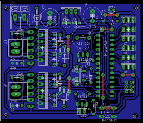
PCB layout design notes
- Select the right component package:
- Make sure you find the components before using them in your PCB layout.
- The component package should have a proper dimension. Not too big compared to your PCB size (e.g. big switches, LEDs, relays) or too small - you can't solder very small SMD components.
- Arranging components:
- The main component (microcontroller, motor driver, or important ICs) should be put at the center of the board.
- Put related components together for the ease of connecting wires.
- Connectors (power, sensors, motors,...) should be put at the sides of the PCB. Then you can connect cable more easily and prevent wrong connections.
- Try to fill your PCB area with components i.e. limit the "blank area" as much as possible.
- 1-layer or 2-layer PCB?:
- Look carefully at your PCB layout. It's always recommended to design a 1-layer PCB because most of your designs are simple. For wires that you can't route totally in the same layer, use jumpers.
- For 2-layer PCB, keep in mind that you have to connect the vias yourself. So, try not to put vias under ICs.
- Wire thicknesses: Since the technician makes the PCBs manually, your wire thicknesses must match the requirements.
- In general, all write thicknesses should be at least 20 mils (~0.5mm) while 25-30 mils (~0.6-0.7mm) are more preferable. With this thickness, you can route a wire between 2 pins of an IC (50 mils).
- (Optional) Power and ground wires should be thicker because they carry more current (~35-40 mils or ~0.8-1mm).
- Wire clearance: Keep wires at least 20 mils (~0.5mm) far from each other and also from pins, vias, and holes.
- Holes: Put holes so you can place your PCB in your system by using screws.
- Use DRC to check errors (configure this function to match the above requirements).
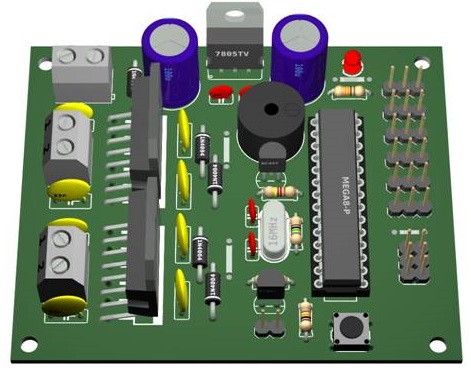
- If you have enough time, can try to render your PCB in 3D by using Eagle3D or EagleUp.
Up
|