

In this section, our printed circuit board will be explained in detail. First, our initial PCB design will be described and discussed. Then, the various modifications and improvements will be exposed, leading to the final optimized PCB layout.
The First Design
Initially, we decided that the PCB would not be on the robot, to have no impact on the weight and the dimensions of the robot. However, as the accelerometer needed to be on the robot in order to measure the acceleration, this would have meant that two PCBs would have to be made:
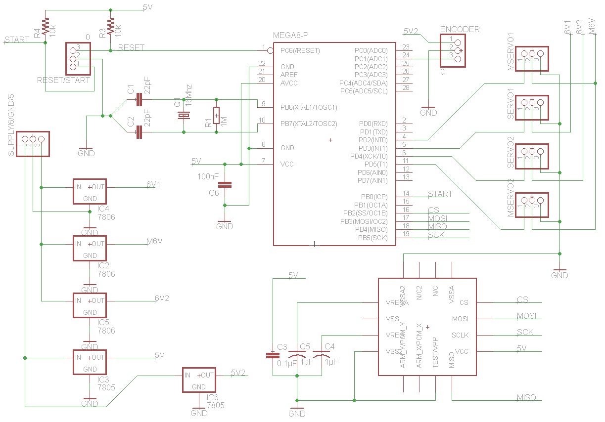
- A small one for the accelerometer only (and the necessary connections to the main PCB), respecting the dimensions of the robot. - A main one, placed aside the robot, containing all the other component. Its scheme is given below.
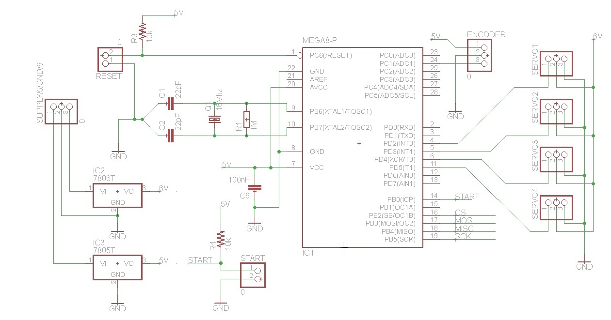
The first step was to choose the microprocessor. We decided that the Atmega328-pu was a good choice, since it is the same as the one used on the Arduino Uno board, therefore eliminating the potential compatibility problems.
Moreover, as the Eagle schematics of the Arduino board were available online, it could be partially copied to implement the essential parts (e.g. the crystal).
To make the scheme, we used the Eagle program. Since the Atmega328-pu is not available in their database, we chose a Mega8P microprocessor, but all the pins were corresponding.
On the left side of the above scheme, we have the reproduction of the scheme of the Arduino Uno. On the right side, we see the 4 servomotors, a Bus for the potentiometer (referred to as encoder because it is an early scheme), a Bus for the accelerometer and finally a Start button (in addition to the Reset button).
Finally, we made two supply circuits for a simple reason; we had to use the highest voltage possible for our servomotors, in order produce the maximum torque. Since this voltage is 6V and considering that our processor can only support 5V, we had to use two regulators: the 7806 (for the 6V) and the 7805 (for the 5V).
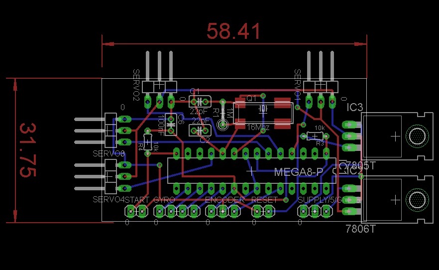
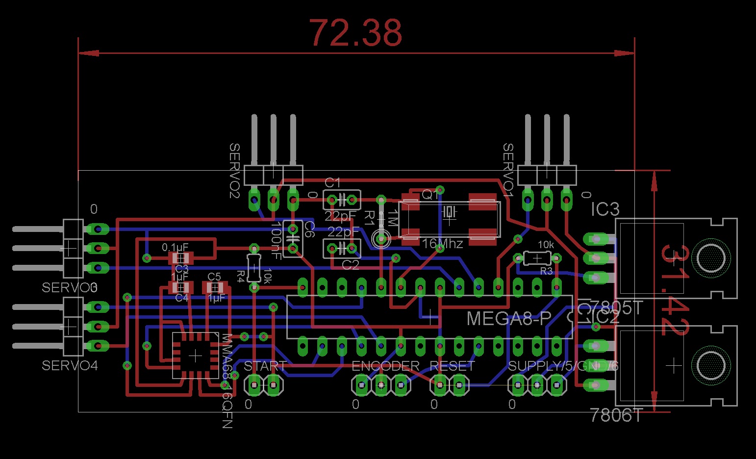
Based on this scheme, a first draft of the Board was made (not optimized yet). As many tracks as possible were place on the back of the PCB
in order to ease the weld.

The Two PCBs in One
Realising that the dimensions of the PCB were quite small, and also because a large number of wires connecting the external PCB to the robot could have hindered its motion, it was decided to include the main PCB on the robot. As a result, the accelerometer could be added on the main PCB, which was a much easier solution.
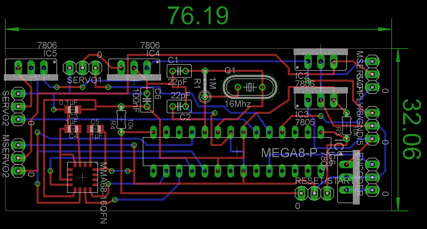
The scheme corresponding to the new PCB is given below.
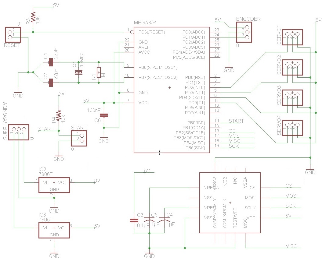
The corresponding board had to integrate the accelerometer and had to be smaller than 80x35mm (because the space on the robot was limited).
Since the accelerometer is surface mounted, its presence increased the number of tracks on the top of the PCB.
One encountered problem came from our voltage regulators, as we were limited by their prices. A quick calculation allowed us to highlight the fact that two regulators were not sufficient to supply a sufficient current to the servomotors. To overcome this problem we simply put several in parallel.
So finally, we used 5 regulators:
- Two 7805 (for the 5V grid) to supply the microchip, the accelerometer and the potentiometer. - The three others were dedicated to the servomotors.
The regulators were designed based on the datasheet of the servomotors, specifying that the currents were of 1500mA and 700mA per servomotor, respectively for the large servomotors and the small ones. It seemed logical to use one regulator per large servomotor and one for the two small servomotors.
The regulators were added as shown on the scheme, where we can observe two +5V tracks (called 5V and 5V2) and three +6V tracks (called 6V,
6V2 and M6V for the microservo). Following this logic, we called the two small servomotors "Mservo".
The Final Optimized Design
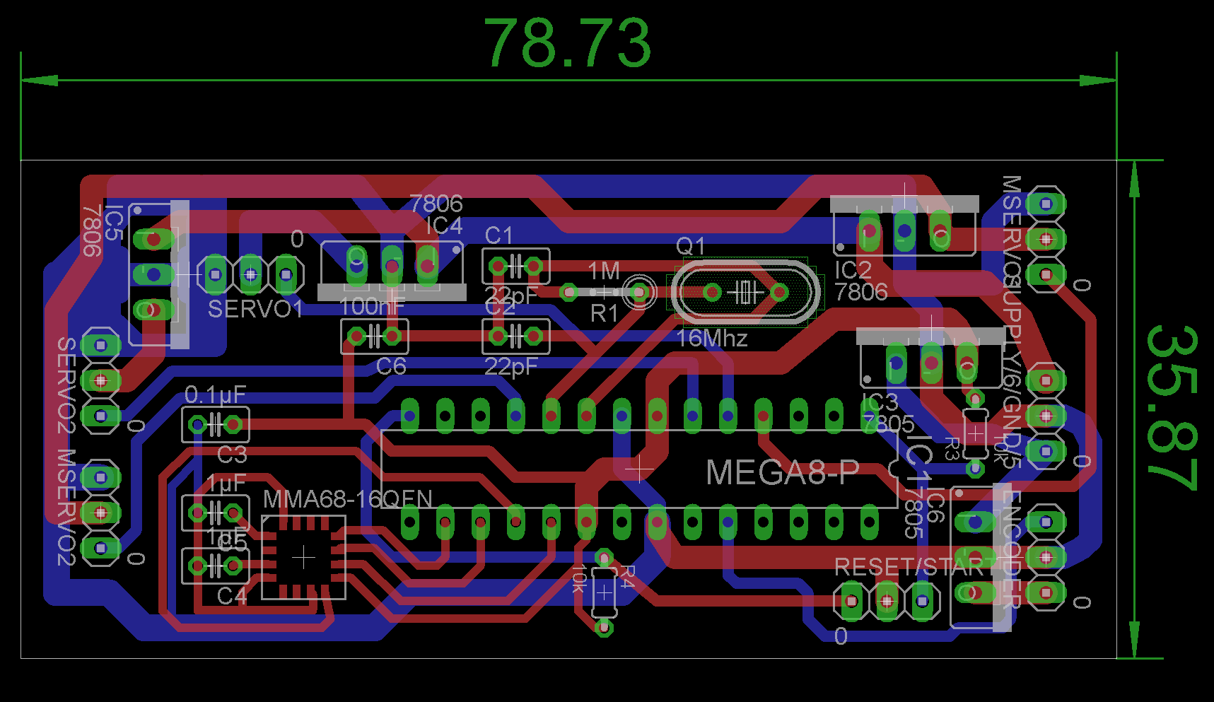
The final step was to dimension the trails in function of the current passing through, by giving them a sufficient width to avoid overheating.
Finally, parallel to these modifications, the VIAs were eliminated. Eased by the change of some "surface mounted" capacitor for "through hole" capacitor, we were able to remove all the VIAs.
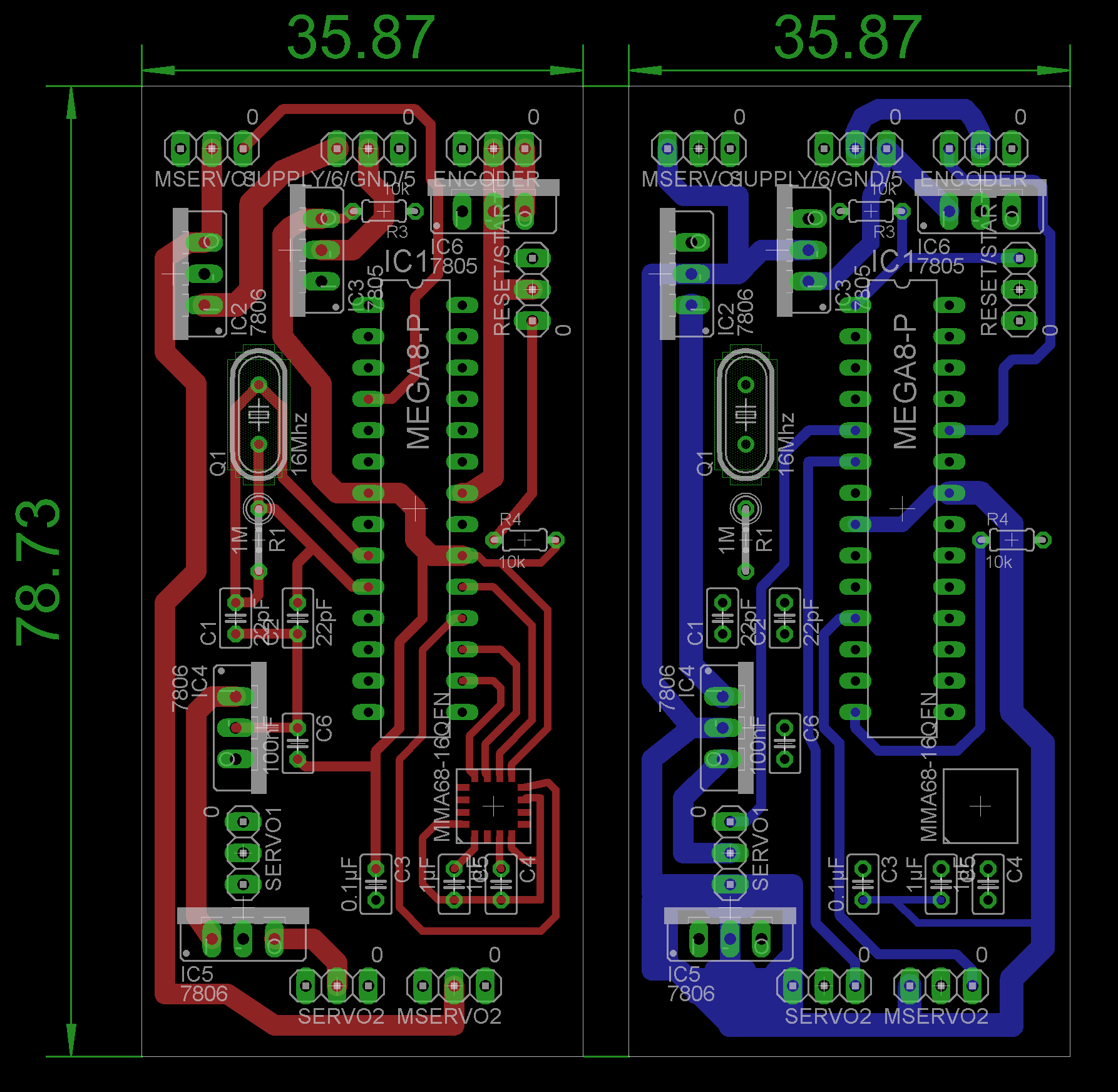
Here is the scheme of the final PCB, which dimensions are: 79x36mm.
To conclude, here is a view of the two separate layers (top and bottom) which allow a better comprehension of the circuit and the real aspect
of the PCB. We can note that all the components are mounted on the top layer.
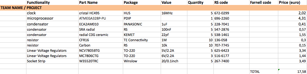
Here is the list of the electronic components that we bought: